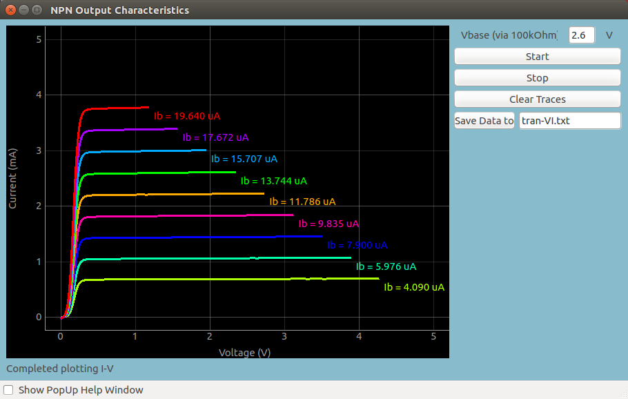
Transistor output characteristics in CE configuration (NPN and PNP)
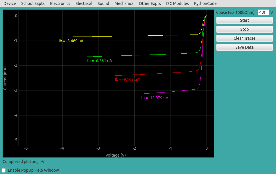
The schematic is wired as shown in the diagram below. The base current is
set by the voltage from PV2, through a 100k resistor. The base voltage is
measured to calculate the base current from Ib = (PV2-A2)/100K. The
collector voltage is monitored by A1. The collector is connected to PV1,
through a 1k resistor. For a selected base current, the voltage at PV1 is
incremented in steps and at each step the collector voltage is measured.
Corresponding collector current is calculated from i = (PV1-A1)/R. The
transistor used is 2N2222, having a current gain of around 200.

|
|
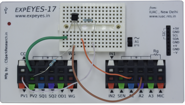
| Wiring Diagram |
Photograph of the experimental setup. Transistor is 2N2222 |
|
| Screen shot of Diode IV characteristic |
Output characteristics of PNP transistor (2N3906) is shown below